Introduction
FPGAs (Field Programmable Gate Arrays) are cool devices that contain internal logic elements that can be reconfigured using what's known as a Hardware Description Language. HDLs (such as Verilog, which I used for this project) may look like normal programming languages at first glance, but work in a completely different way, because you use HDLs to describe the actual hardware that you want your FPGA to configure to, which may be logic elements such as AND, OR, NOT gates, adders, etc.
In this blogpost, I will outline how I implemented hardware for I2C communication between a DE0-Nano FPGA and a ST7567S based 128x64 LCD display. Then I'll show how I used this implementation to play a basic game of Pong.
Planning
To keep things simple, I decided to maintain a 128x64 frame buffer on the FPGA. I would then be able to implement a module that repeatedly iterated over this frame buffer and send pixel data to the ST7567S over I2C.
This design would allow writes to the frame buffer without the need for any clock synchronisation with the module that handles the I2C communication. This should hopefully make it easier to optimise the I2C clock speed (hence, maximise the refresh rate of the display).
I2C Implementation
Again, to keep things simple, I skipped a full I2C implementation and instead went with only what was required to write data to the LCD. The ST7567S IC internally contains a DRAM frame buffer that supports both read and write. Since we are maintaining a frame buffer on the FPGA, reading from the LCD frame buffer is not necessary. So, we only need to implement a write I2C transaction.
Specifics of interfacing with the ST7567S over I2C is detailed in the datasheet (see Links section below).
Signalling
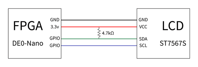
I2C consists of two open-drain connections, SDA and SCL. SCL is the clock, which in this case will only be driven by the FPGA, so SCL doesn't strictly need to be open-drain here.
However, SDA will be driven by both master and slave. So on the FPGA side, a tri-state buffer is required to output either a high-impedance state (Z) or a low state (0) on the SDA line. SDA will also need a pull-up resistor to 3.3V.
As such, the connections between the FPGA and LCD will look like this.

Transmitter Module
To keep things short, I won't cover the low level details of how I2C works (there are great resources available elsewhere). At a high level, the write I2C transaction consists of the following parts:
- Start condition
- Slave address
- Receive ACK from ST7567S
- Register address
- Receive ACK from ST7567S
- Data byte to save to register
- Receive ACK from ST7567S
- Stop condition
The I2C transmitter module (i2c_transmitter.v) has been implemented using a Finite State Machine (FSM). I found that a good starting point was to create one state for each part of the transaction above. I then added a few more states to handle the stop condition correctly.
Initialising LCD
With the I2C transmitter ready, the next step involves actually sending data to the LCD. Before we can start drawing anything to the display, the LCD has to be initialised. For this, a sequence of data is written to the LCD to reset it, configure LCD drive parameters, then enable the display. See the source code linked below for a full explanation of all static data that is sent during initialisation.
This static data is stored and sent to the I2C transmitter module from the i2c_data_static.v module. After this data transfer is complete, the init_complete flag is set, which switches the data source for the I2C transmitter from the static data to the frame buffer.
Frame Buffer Implementation
After the initialisation data is sent to the LCD, the frame_buffer.v module takes over to send data to the I2C transmitter. This module simply iterates through the frame buffer and continuously sends display data to the LCD.
Optimisations
To get the fastest update speed possible, I had to perform some optimisation on the main update cycle. Rather than setting the page (row of bytes) and column before sending each byte of data, the Read-modify-Write mode of the ST7567S was used, which auto-increments the column pointer when a byte is written. Additionally, incrementing the page number is only done when starting a new row.
With these optimisations, I was able to achieve a display refresh rate of ~14.7Hz, with a corresponding SCL frequency of 890KHz. This decently fast for I2C, and I was likely limited due to the wires and breadboard connections I was using for my test setup.
Further optimisation is still possible, as the ST7567S supports burst writes (writing multiple bytes in single transaction). Using this would allow for faster writes as the additional overhead of sending the start and stop condition would be removed. I decided against implementing burst writes for this small proof-of-concept project to keep things simple.
Pong! 🏓
With the frame buffer functional, I needed something to test the whole system. I chose to implement a basic version of the Pong game since it's quite simple.
The process.v module implements the game, which essentially involves moving through each column of 64 in the frame buffer, and for each column, setting bits to 1 where a paddle or the ball is found. This module can run at arbitrarily fast clock speeds in comparison to the I2C logic, as the frame buffer writes are independent of reads.
The user inputs to move the paddles are from four pushbuttons (with corresponding pull-down resistors) connected to four GPIOs on the FPGA.
Conclusion
That's it! Feel free to check out the Verilog source files in the Links section below.
Links and Downloads
Links
Downloads
- ST7567S Datasheet → ST7567S.pdf